Using an ESP8266 to interface with HDDs
In one of my draws, I have a bunch of old HDDs from over the years, I was looking for a file related to an ond project I had created back in 2009, when I realized that old my older HDDs have an IDE/PATA interface and I will not be able to read them with my SATA adaptor. Since I wanted my files right away, and did not have a store nearby to get an adapter, I decided to make my own IDE/PATA reader and ended up hooking it up to an ESP8266 too.
I started by reading up on the functionality of PATA storage devices^[The ATA3 standard can be found here], I looked into the pinout of the 40-pin PATA connector and checked to see in the project was possible. Since this was an older technology, I was glad to find that the pinout of the PATA port is simple, and had a great chance of working^[ATA3 Standard chapter 4.1 “Signal summary”]. A PATA interface has 40 pins, but to get the device operational and read data of of it, only 24 pins really need to be connected. There are 16 data lines and 8 control lines in the flowing configuration (signals marked with a leading / are active low):
- /RESET - HDD reset line.
- /DIOW - Drive I/O write strobe.
- /DIOR - Drive I/O read strobe.
- DA0..DA2 - 3-bit register address lines.
- /CS0../CS1 - Chip select lines, used with DA0..DA2 to select registers.
- D0..D15 - Data lines, used for data transfer and register read/write (lower 8 bits).
There are many more control lines that may be added, such as interrupts, DMA, Activity indicator and more, but keeping it down to 24 lines reduces complexity and the amount of I/O pins needed.
So I knew what signals I was going to use, but how are the signals used? So, in brief, the PATA device has the a number of registers, which can be accessed by combining the /CSx and DAx signals. Each registers meaning depends if the device is being written or read from. All the registers and functions are described in the ATA3 standard, Table 6, and section 5.2. For example, the first thing that needs to be done when the drive is powered up, is to initialize the device this is done by waiting for the BSY bit is clear (bit 7 of status register) and the DRDY bit is set (bit 6 of status register). After the device is initialized, a IDENTIFY DEVICE command might be sent, in order to gather some information about the drive itself (section 7.7). After the command is issued, a 512 byte (256 word) structure can be read from the data register and be used to identify the device type, model, manufacture and size. Once information is available, a sector(s) can be read by setting the appropriate addressing registers and sector count, issuing a READ SECTOR(S) command (section 7.18), and if everything goes well, the data can be read from the data register. Well, that’s some basic operation examples, there us much more to cover for good operation, and the ATA standard is a good place to start.
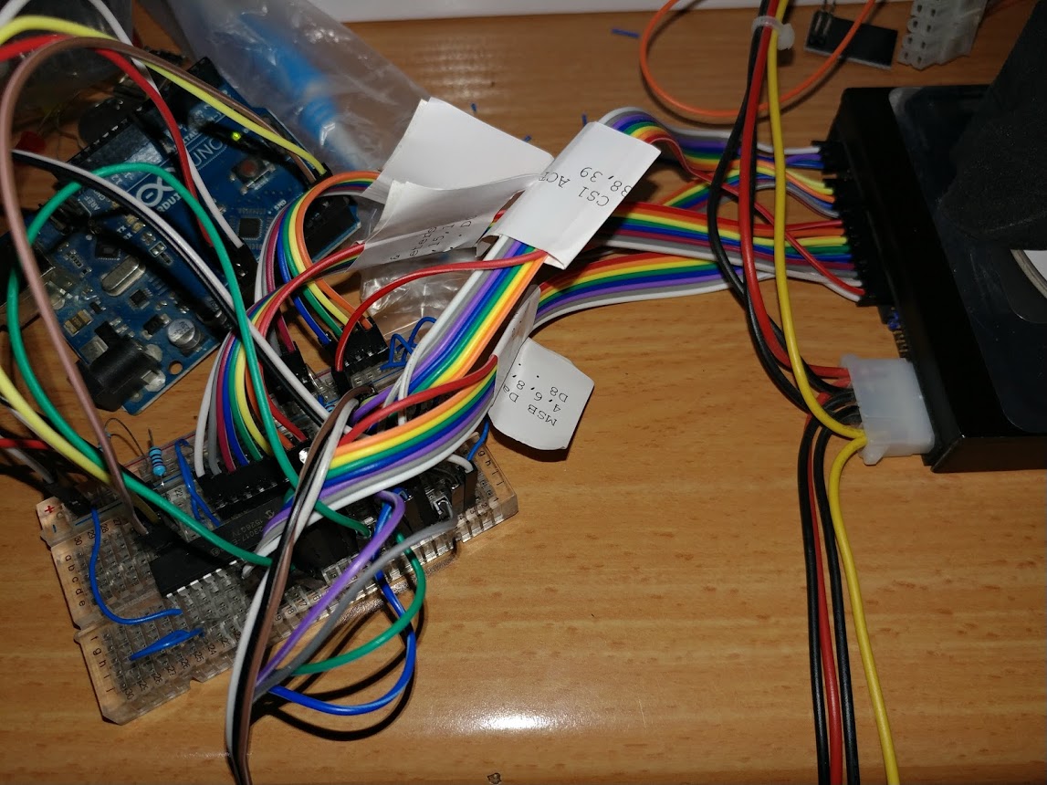
After the the basic operation is understood, the next step in the process was to setup all the connections to the drive. I attempted to start simple, with just an Arduino, but my UNO only has 14 I/O pins and I need at least 24. In order to get to 24 pins, I decided to connect 2 I/O expanders on a breadboard and work with them. The I/O expanders selected were chosen were a 16 bit MCP23017 and a 8 bit PCF8574, both have an I2C interface and can sit on the same bus, reducing the amount MCU I/O pins to 2. For the power source (these drives require a 5v and 12v rail) I used an old PSU I had lying around and shorted out /PS_ON to ground to turn in on without a motherboard. It took me a while to try and get the setup to work, and it did work sometimes, but most of the time I had random issues that I could not understand. After some time, I connected a logic analyzer to some of the PATA pins, and saw there was considerable noise and interference on the lines. At the point, it was clear it was not going to work on a breadboard and had to find a different solution (Also, this was the point where it went from a project out of necessity to a project out of curiosity).
The solution came in a form of a custom designed and printed PCB, with the most basic layout:
- 4 pin header for power and I2C bus.
- 40 pin male IDE cable socket.
- x1 PCF8574.
- x1 MCP23017.
- x2 pull-up resistors.
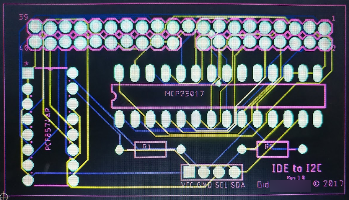
This was not an optimal or good design in any way, shape or form. I did not have any resistors on the data lines, no diodes for protection, nothing. As this was my first PCB, I managed to mess up the silk-screen labels (but not the traces, thankfully) . In hindsight I should of added a 74LS04 (hex inverter) and routed some of the active low signals through it, so the software side should not need to deal with the logic level stuff and they are considered active high in the code. This was also the time I decided to switch from using a Arduino to using an ESP8266 (01) module as the MCU, this allowed me to use Micropython for rapid testing, and worked will since i2c only needs 2 I/O ports. The only downside to using an ESP8266 was, that there is not hardware I2C driver on the chip, it’s all done in software.
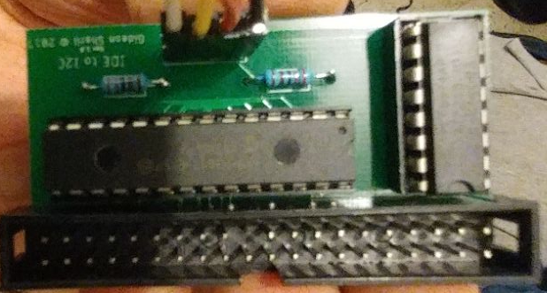
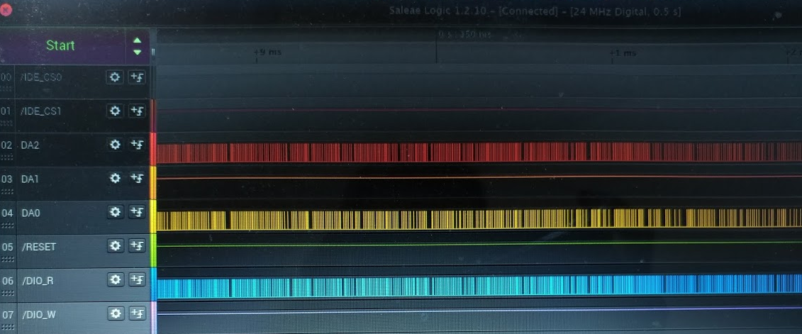
After connecting it all back up, to my surprise, this board actually worked. After a second check with a logic analyzer, there was no noise present on the control lines and I was able to connect to the drive, I was still fumbling around in the datasheet to get the device to respond to read requests, but there was hope.
The first thing to do with the new setup was to setup a python class to represent the the two I/O expanders, each class has a general setup methods to scan and find the device (at the default I2C address), set I/O direction, and toggle I/O port. After testing the I/O expander woked with an LED probe, I worte a class that represents the IDE/ATA interface to the device. The class provides methods for reading and writing control registers, reading and writing data, printing the drive registers for debug, and other helper functions such as drive initialization, setting LBA addressing, resetting, and going into sleep mode.
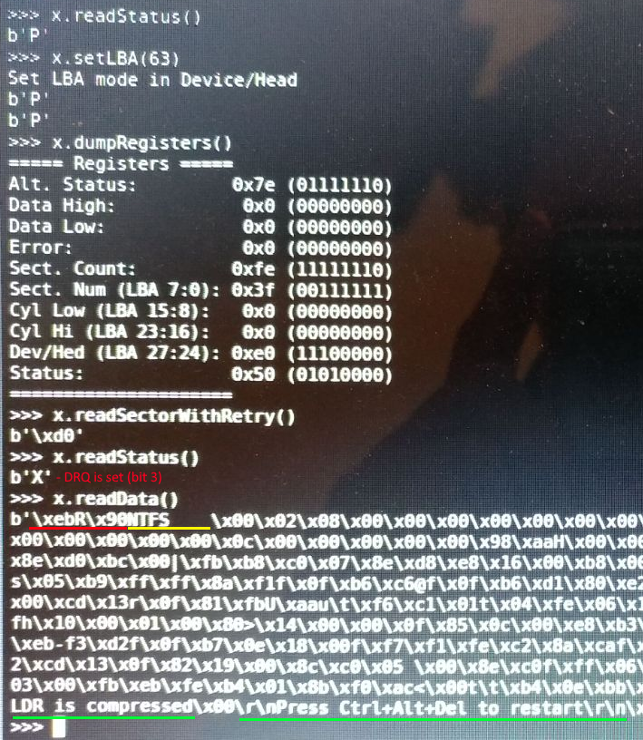
After some debugging I finally managed to read the first sector of the disk (the boot sector), Looking at the output from the drive, It was clear this was the boot sector from the boot signature (0x55 0XAA) in the last 2 bytes. At offset 0x163, 3 null terminated error messages can be seen, and at offset 0x1BC the partition table can be seen. To make sure this was not a fluke, I also read the 0x3f (63rd) sector of the disk, which is the first sector of the first partition (found from the boot sector), this, as expected, was the NTFS partition boot sector, which started with \xeb \x52 \x90 which in x86 assembly would be JMP 0x52; NOP or, in english, a relative jump 52 bytes forward, jumping to the NTFS bootstrap code (at offset 0x54). The following image demonstrates the the findings, the first thing to do was to check the status registers and see if the device was responding, after a valid response was returned, the LBA was set to 63, which the first partition of the device (this is an older disk so partition 1 is at offset 63, today the first partition is usually located at sector 2048). After the setup, a register dump is done to make sure everything is setup correctly, and finally, the readSectorsWithRetry read the sectors requested, a status check is preformed to check that DRQ (Data Request) is set in the status register, indicating the drive is ready to transfer the data. finally, readData is called in order to transfer 256 words from the 16 bit data bus to the host (a total of 512 bytes - 1 sector). In red is the JMP 0x52; NOP, in yellow is the OEM ID and in green is 2 strings that can be seen as part of the 512 byte bootloader, especially the string Press Ctrl+Alt+Del to restart gives away that this is the bootloader.
I think it’s time to wrap up this post, I will follow up in another post about using the setup described in this post to read and parse the FAT32/NTFS file information. Also, you can find useful references in the footnotes.