Testing PCB Etching at home
For far to long I have wanted to make PCBs at home. Even though there are many cheap PCB manufacturing plants in china, it takes time for the order to complete, and without paying an extra 20$ for expedited shipping (which can be 10 times the cost of the PCB), it takes weeks to arrive in the mail. For these reasons, I really want to find a way to create basic POC PCBs at home for, even if they cost a bit more than the cheap china ones, and are poorer in quality.
I started by reaching thr PCB etching process, it turns out, there are only a few steps to the process, an I can eliminate some of them. The first decision to make was to choose a manufacturing method. There are many PCB manufacturing methods for home, but the main 3 are a follows:
- Etching copper clad boards with acid.
- Milling copper clad boards with a CNC.
- Printing conductive material with either a 3D/printer.
The only real option for me is the first, using acid to etch copper clad board. The reason for that is that I have no access to a CNC mill, and I don’t own a 3D printer. There is a way of using a regular printer with a conductive ink cartridge, but the traces will be to thin to carry any high currents I might need. So option 1 it is.
In order to etch boards with acid, there are 3 main steps that are taken, and a few additional steps fo finishing:
- Mask the areas of the board to be etched.
- Etch the board in a acid solution.
- Wash.
- Add solder mask to protect copper and help solder flow.
- Drill holes for through hole components.
In order to mask the board in step 1, there are a number of ways to do this. The preferred way is to use a UV curable photoresist, this requires a UV lamp to cure , and if has the potential of going wrong if the photoresist is not stored properly (and may cure on it’s own). The second popular method is to use a laser printer to print the circuit paper, and the use a hot source to re-melt the plastic toner and transfer it onto the copper clad board. I opted to use the second method as the parts are availabe to me quickly if not in stock (toner, printer, paper).
The next thing I had to research was the etching solution. In most cases, Ferric-Chloride is used as the enchant. Unfortunately, this is not an acid that can be bought off the shelf at my location, and another downside to ferric chloride is the color, a dark brown/red that will stain anything that it splashes on/contacts. After more research, I found that Hydrochloric acid can be used with some Hydrogen Peroxide. As it tuns out, hydrogen peroxide can be found at any chemist’s shop and the hydrochloric acid is used by construction workers as a cleanup solvent. I got some 3% hydrogen peroxide and 30% hydrochloric acid and in order to remove the toner from the PCB after etching, I also got some acetone, but alcohol can be used too.
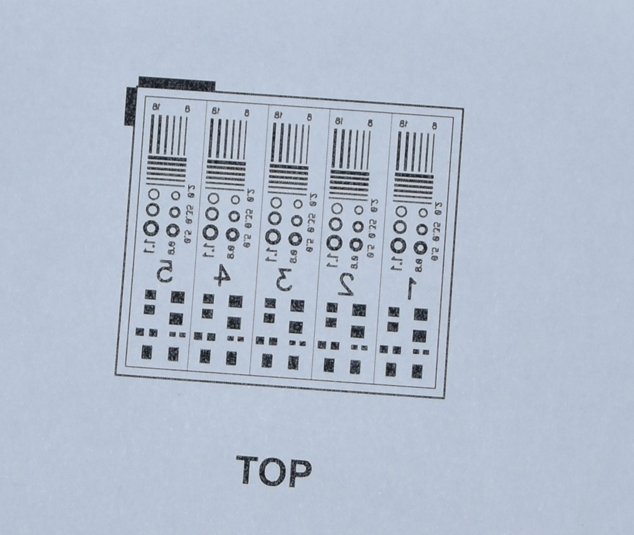
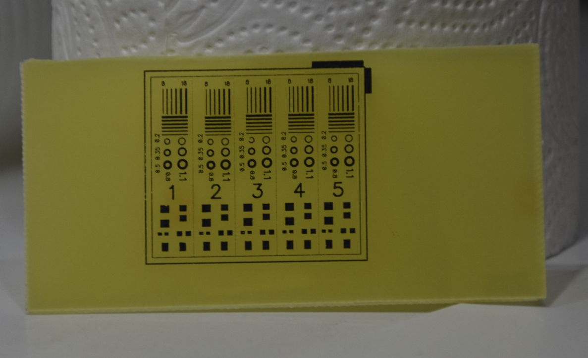
I decided to do a test print as I wanted to test the accuracy and limits of the method I was going to use. So I found a test pattern online with various hole sizes, track widths and SMD pad sizes. I printed the pattern (in draft mode) onto a piece of paper and checked it for size and made sure it came out mirrored as it will be transferred onto the copper. It looked good.
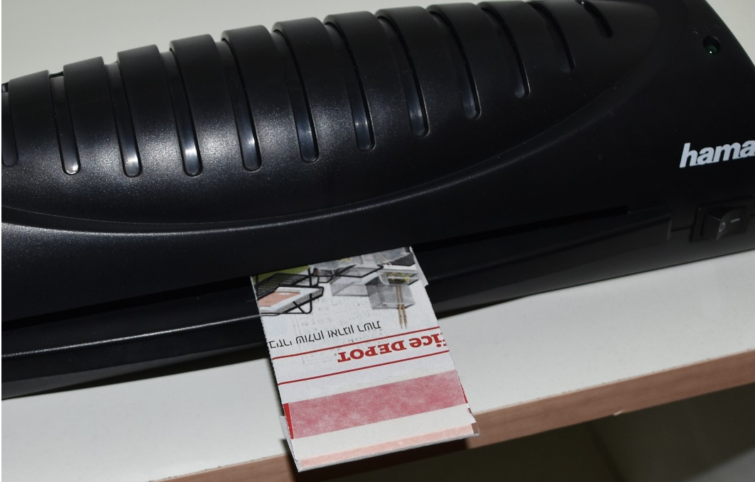
After I had the pattern all figured out, I too a piece of thin, cheap chromo paper that I cut out of a products catalogue and printed the pattern onto that. The reason for chromo paper is that it is not as rough and will allow the toner to transfer more easily to the copper, the reason I used thing paper, was fo the so it will disintegrate faster in waster when needed to peeled off.
After I had the printed pattern on the cheap paper, I cut a piece of copper clad board the same size as pattern, cleaned it with soap and water, then I stuck the printed paper face down onto the board. I used some masking take to secure it from the top and bottom to the board, so it did not move in the next step, which was to heat the board up and transfer the toner to the board. Any hot, flat surface can be used to transfer the toner to the board, I used a thermal laminator machine for the job, but an iron could work as well. Since the copper board is thick and has a substantial mass of copper, it absorbs the heat very well, so I passed the board thought the machine several times, flipping which face was up every other time. I passed it through the machine approximately 12 times, 6 on each side.
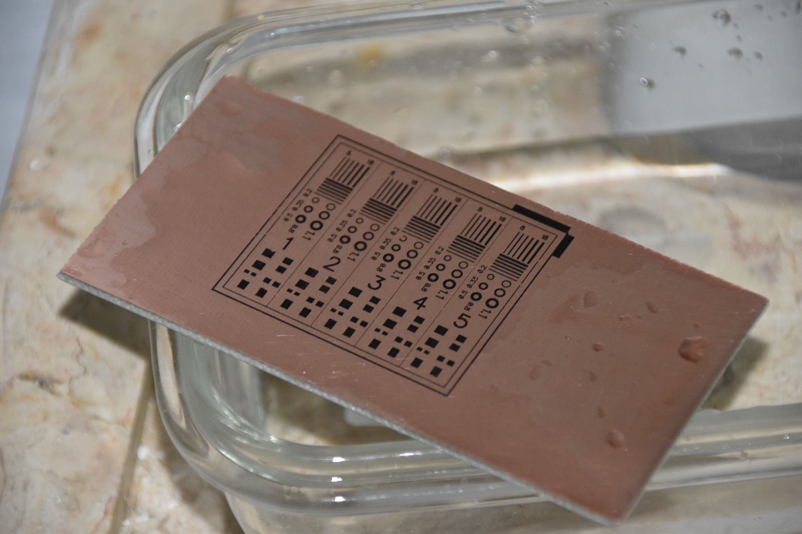
Once the board cooled, I put it into a water bath and let it soak for a few minutes, then, I carefully peeled the paper off the board, and gently rubbed the toner area with my fingers, releasing any paper residue on the face of the board. It’s important not to use a scrub pad or brush that may scratch the toner, ruining the mask. I then let it dry out and inspected the transferred mask. I did not fix any issues with the transfer I had, since I wanted to check the limits of the “vanilla” mask, but if any gaps are found, it should be possible to touch up with a sharpie pen.
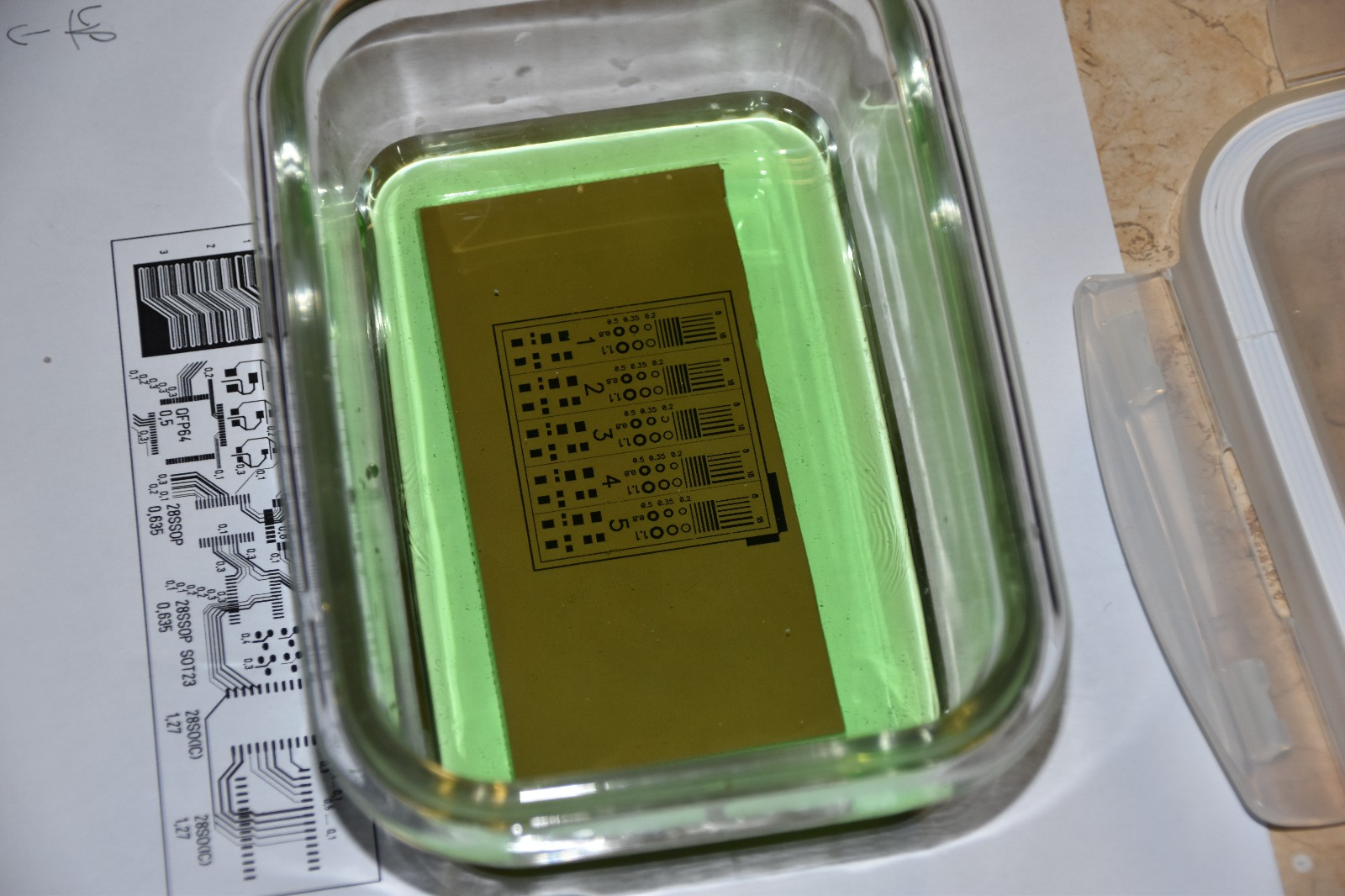
After the board was dry, I prepared the acid solution. I added 1:1 parts of hydrochloric acid and hydrogen peroxide and mixed them well. I did this a a well ventilated area, and then took the board, a container and the solution outside to an open area. I put the board into the acid and let it sit. The nice thing about the hydrochloric acid method, is that the solution is clear, unlike the ferric chloride which is opaque. After sitting in the solution for a couple of minutes the liquid started turning green, and as time went on the color got deeper and deeper. The color change of the solution is a good sign indicating the copper is being dissolved into the solution.
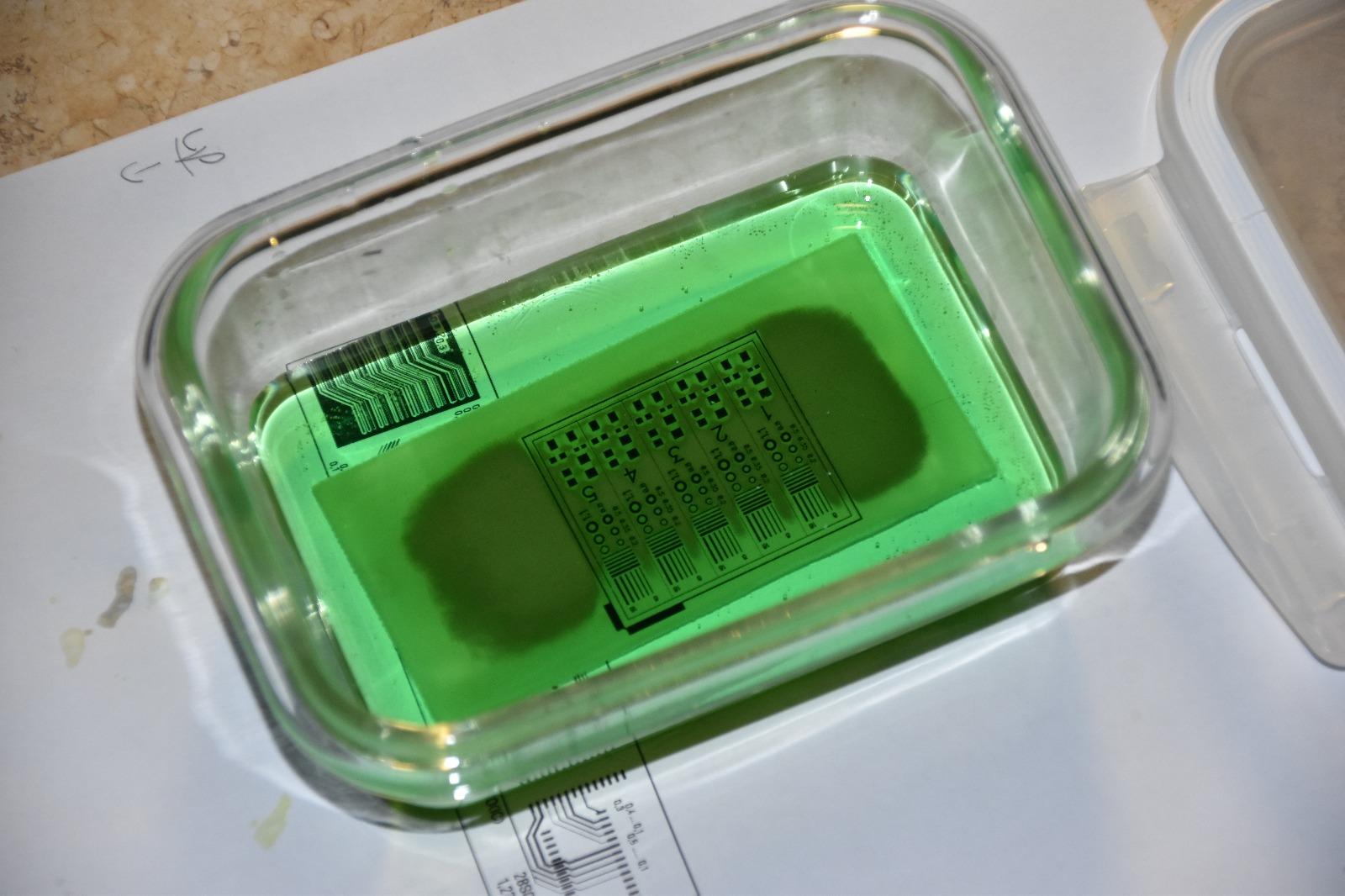
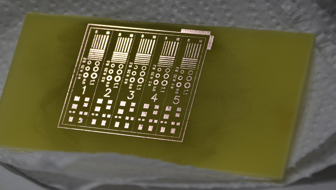
After I could not see and more copper on the face of the board, it was time to take it out and give it a rinse. I made sure it was thoroughly cleaned before attempting to touch it with my bare hands. I then again inspected the toner markings to make sure they held up to the process. There wre some breaks in the toner, but they were there before the etch, so I didn’t expect it to be etched to perfection. After most of the copper is gone, the yellow backing board color can be seen.
After another drying with some paper towels, It was time to remove the toner mask and see if there was any copper left behind, in the right places. I used some paper towels and acetone and gently rubbed off the toner. The acetone is a solvent and dissolves the plastic toner. I did learn that the toner gets smeared al over the nice clean board when running it, so maybe using a shallow batch will yield cleaner results, nonetheless, beautiful shiny copper traces started to emerge from the toner darkness and I could no be happier with the results. It does seem that the very fine details did not do well mostly the 0.2mm holes but the 0.35 and upwards loos very good, and the traces, they are all mostly just fine. I did also test them with a multimeter, and most tested OK.
In conclusion, the results I got were beyond my expectations (especially for a first time), the materials to do th etching are inexpensive and accessible to me, the process itself is fast and not much preparation time needed. And if that was not enough, the acid solution stores well and can be rejuvenated with a touch of hydrogen peroxide.
Until the next time, have a nice day.