Reversing a CANbus odometer filter/manipulator
Intorduction
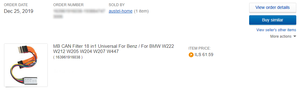
A while back, I watched a video on YouTube by Big Clive in which he showed and tore down a device that is used to manipulate the mileage displayed on an odometer of a car. The teardown was very interesting and was very informative on the design of the device. The video, titled Naughty CANbus odometer “interface”. (Fakes mileage.) did a great job of looking at the hardware side of the device, but the software functionality of the device was only based on speculation. When I saw the video, I decided to find the device for sale, order one and take it apart and take a look at the software side dof things. As I did not have any information on how to purchase the device, I started by searching Google for various keywords that fit the devices functionality and the silk screen printed car models that appeared in the video. I got multiple, different devices in the search results, I switched to using the image search results and tried to find a device which visually matched the the one in Big Clive’s video as close as possible. After some searching, I found that the device is commonly sold on eBay under the name “MB CAN Filter 18 in 1”, there are a few versions of the device for sale, but the images helped identify the specific device featured in the video. After I was positive I had the correct device, I ordered one off of eBay and waited for it to arrive. I guess I was not the only one to order this device off of eBay as when the device was shipping, a significant amount of eBay listings for the device had been taken down, maybe due to the exposure Big Clive’s video. In case you want to look for the device yourself, I have posted an image of the purchase order that I made, as the listing itself is no longer available.
It took a whole two months for the device to arrive from China, At first I was anxious that the device was stopped at the border by customs, as using this kind of device is highly illegal, and is a criminal offence at my location. I was relieved once the device arrived without a mysterious phone call from customs or sudden charges/investigations launched (car parts imports are heavily regulated). I guess that the COVID-19 situation in China may have caused delays but if you do order such a device, remember that it is used for illegal activity and may cause trouble at the import stage.
Invastigating the hardware
Once I had the device in hand, I took a knife and peeled off the black head-shrink tubing that was protecting the PCB. There was also a sticker attached to the heat-shrink tubing with what looked like a version number of some sort, instructions (maybe? in was chinese) and different car model numbers. After I had the bare PCB in hand, I could inspect it visually and compare it to the device that was presented in the video. I was glad to see that it was an exact match to what was presented and that even had the same car model jumper set in the configuration area. As the video does a good job of showing the PCB and all of it components, I will not break down the whole board in writing and will only provide an overview of the components, with emphasis on the components that are of interest for the task of reversing and understanding the firmware.
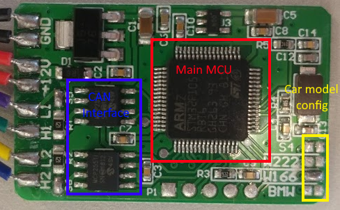
As can be seen in the image above, the main component on the device is an STM32F105RB micro-controller. This micro-controller is a 32-bit Cortex-M3 ARM processor and is rich in peripherals. The STM32F105 has a maximum clock speed of 72MHz, flash size is between 64KB and 256KB and a SRAM size of 64KB (depending on the configuration). It supports USB, I2C, USART, CANbus, I2S, SPI and has a ton of timers and GPIO pins, some of them even have hardware Ethernet available. The other two interesting chip is the dual Microchip MCP25511, this device, described in the data sheet as a “High-Speed CAN Transceiver” sits between the STM32F105 and the CANbus lines. There are two CANbus transceivers, one is connected to the ECU (the cars computer) side and the other is connected to the instrument cluster, each MCP25511 is responsible for the communication on its side of the CANbus. Before I proceeded, I hooked up at the device to a logic analyzer and oscilloscope to check the operation of the device. I used a PSU to supply the device with 12v and watched the 2 CAN buses carefully. After some long captures and waiting for the scope to trigger on any communication, I came to the conclusion the device is not actively sending out it’s own CANbus frames. I also thought of using some CAN to USB or Arduino/RaspberryPi to send my own CAN messages through one end of the bus, but I did not have the required hardware to handle CAN on hand (bit-banging is not reliable due to timing issues).
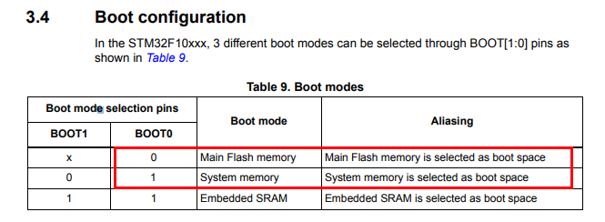
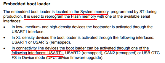
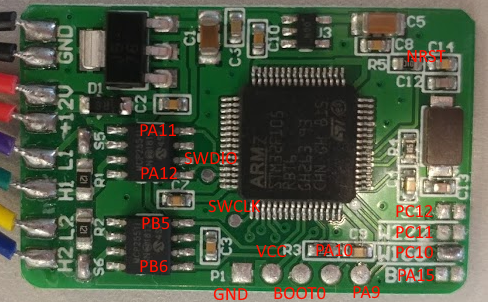
My next step into investigating the device I needed to check out all those test pads and connection. The fist thing to do is to find the datasheet for the STM32F105 and the MCP25511. Using the STM32F105 datasheet and a multimeter, the connection can be traced out and matched to the pins of the micro-controller. I started by mapping out the rwo of test pads on the long edge of the board, I added text on a photo of the board so it will be easier to follow (attached below). I found the connections to be almost be standard, GND (ground), 3.3VCC for power, a pin named BOOT0, and what appeared to be two GPIO pins (PA10 and PA9). Reading through the datasheet, it seems to be that PA10 and PA9 are also used for the Rx and Tx lines of the USART1 peripheral, is there a console on this device? Well not exactly. The one test pad I could not figure out was BOOT0, Looking up the datasheet for the functionality of thr BOOT0 pin, it appears to be to select some boot configuration. There are 3 boot configurations that can be selected using pins BOOT0 and BOOT1, in the case of the STM32F105 LQFP64 only BOOT0 is available which means that only two boot configurations are available on this device. The fist boot mode, is when BOOT0 at logic low (grounded) the system will boot from the internal flash memory, if BOOT0 is set to logic high (3.3v) it will boot to “system memory”, which further down the datasheet is described as an embedded bootloader to reprogram the flash memory. And how one interacts with this embedded bootloader? using USART1 of course (pins PA10 and PA9). So in theory, the 5 pins mapped out alone will grant access to the flash (at least for reprogramming and erasing).
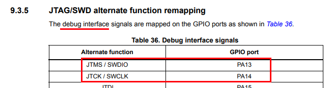
All that was only the 5 pads on the edge of the board, but what about those other 2 test pads dotted in the centre? Well, Good news everyone! I traced them back to pins SWCLK and SWDIO. Reading through the datasheet again, and some more searching shows these pins are used for the SWD protocol, which is basically a debug interface for the device, just like JTAG. SWD stands for “Serial Wire Debug” and the SWCLK pin is used for clocking date in and out of the device, while the SWDIO is used as a bi-directional data line. While the bootloader serial interface and the SWD interface exposure is great news, more reading in the datasheet and technical notes for the STM32F105 reveals that there is also a code protection mechanism that also has the option to mass erase the flash on a failed readout attempt, that can be bad.
Even though I have mapped out the different debug/flashing interfaces of the device, I continued and mapped out the each of the car model configuration jumpers, on the one side, all the pads are grounded and on the other side, the pads are hooked up to GPIO pins of the micro-controller, when a specific GPIO pin is grounded with a solder bridge, it tells the micro-controller the type of car it it plugged into and the device can operate with that specific car model parameter. The 4 model selection pads are mapped to PA15, PC10, PC11 and PC12. In the case of the device that was shipped to me, the Mercedes W166 car model was selected. There was two other things I wanted to map out, the connections to the two CANbus transceivers, and a signal named NRST for the SWD interface. First, the CAN transceiver, one is connected to PA11 (also named CAN1_RX) AND PA12 (CAN1_TX), and the other is connected to PB5 and PB6 which is CAN2_RX and CAN2_TX respectively. Unfortunately, the NRST line did not have a proper test pad to connect to, so I located at handy place to solder a wire, it just happened to be between a resistor and capacitor on the board.
Dumping the flash
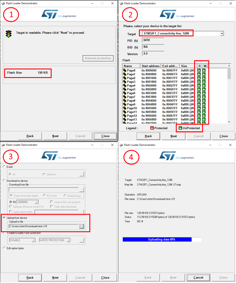
Now that I have all of the hardware mapping out of the way, it’s time to connect up to the device and try and get the code out of it. I soldered on some wires to the test pads and started to try my luck. I decided to start with the serial bootloader interface as I did not have a ST-Link debugger available (used for the SWD interface), So I ordered a STM32 Nucleo development board (it has a built in ST-Link) and while waiting for the dev board to arrive, I started working on the serial interface. The first thing was to connect up the device to a standard Serial-to-USB (3.3v) and connect it to my laptop. In order to get the bootloader to load and not the flash, I connected the BOOT0 pin directly to the 3.3v pin on the serial adapter and hoped I did not blow anything up without a resistor. After some searching, I found the application notes document detailing the protocol of the STM32 USART bootloader. I did also come across 2 tools that can be used to dump the flash data from the device, the first called stm32flash and another, more official one (which works with windows) called Flash Loader Demonstrator. I tried both tools and both of them seem to work equally well, the Flash Loader Demonstrator was really nice and useful in that it is an official tool and shows the protection status of the device before any read attempt. I was glad to see that the device was not protected at all, allowing full access to the flash (read and write). Unfortunately the downside of using the official tool is that it dumps the flash in hex form (Motorola SREC S19) and did require an additional processing step after the dump file was created in order to convert it to binary form, but this was achieved easily using the objcopy tool from the ARM cross compiler toolchain which is also available for windows (arm-none-eabi-objcopy --input-target=srec --output-target=binary input.s19 output.bin).
Static code analysis
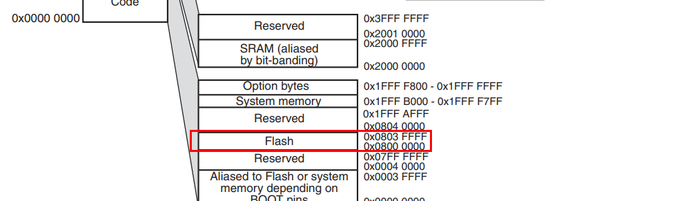
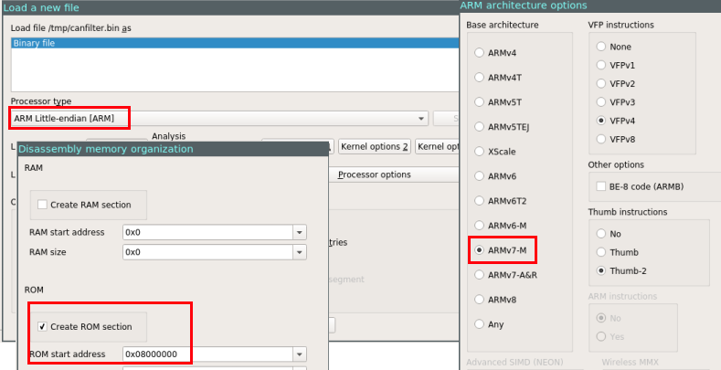
With the flash is in hand, I needed to load it into a disassembler. My disassembler of choice is IDA, when loading the binary, I set the processor type to “ARM Little endian” and in the processor options, I changed the instruction set to be “ARMv7-M”. I disabled auto-analysis and continued to the memory layout. Looking at the images above, it’s very noticeable that the page start address is always between 0x08000000 and 0x08000000+128KiB, looking at the datasheet (section 4, Figure 5), a diagram of the address space is presented, as can be seen in the diagram, the addresses from 0x08000000 to 0x0803FFFF belong to flash. So in order to load the binary image correctly in IDA, a ROM section needs to be created that starts at 0x08000000 the size of 128KiB. If really wanted, a RAM section can also be created as presented in the memory mapping from 0x20000000 to 0x2000FFFF. After setting up the memory layout, IDA can proceed and load the flash dump.
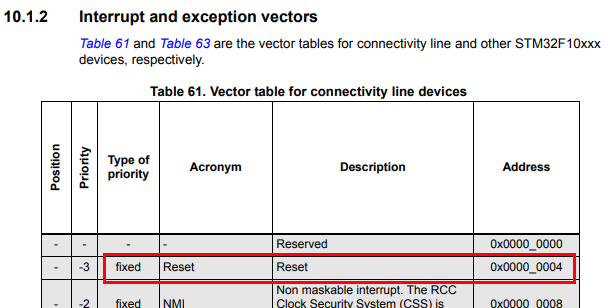
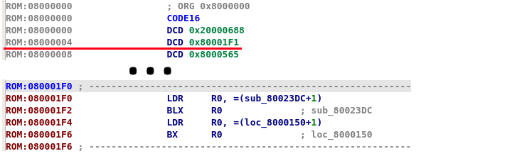
Since the flash dump is not in any recognizable format, IDA will not be able to detect the entrypoint automatically, this is why I disabled auto analysis while loading the dump. So where to start? well, just like in my post about the switcher firmware analysis, micro-controllers have a reset address that they jump to upon startup. This reset address is part of the interrupt vector table and depending on the architecture, it starts at a known address in memory (and may be relocated later by the user code), all that needs to be done is to find the address of the vector table in addition to the offset of reset vector itself. In the STM32F105 reference manual, section 10.1.2 (Interrupt and exception vectors) the vector table can be found with the name, description and address of each interrupt vector. As can be found in the table, the interrupt vector table starts at offset 0x00000000 and the reset vector itself is located at offset 0x00000004, making the actual reset vector 0x08000004 as the flash starts at 0x08000000. Looking at the value at location 0x08000004 in IDA shows 0x080001F1 which is an address that appears to be valid (in the 0x08000000+0x3ffff flash range). There is something interesting thought about that address, if we try and convert the instruction at address 0x080001F1 to code, IDA just fails with the message Command "MakeCode" failed. To understand the failure, the answer is in the address itself, the ARM architecture has 2 different instruction sets, the first is ARM and has 32-bit wide instructions, the second is THUMB which is 16-bit (sometimes 32) wide instructions. In order to distinguish between ARM and THUMB instructions, the LSB of PC (program counter) is used, if the LSB of PC is 0 then it’s running in ARM mode and if the LSB is 1 the instruction are interpreted as THUMB instructions. Whenever the code branches or loads an address, if the address’s LSB is 1 the ARM core will switch to THUMB mode, but no matter if running ARM or THUMB instructions, the LSB of PC is discarded when fetching the instruction. In the case of the code of the STM32F105, since this device is from the Cortex-M family, it only supports THUMB instructions. And that is why branch addresses loaded into PC will have the LSB set to 1 (more info on the subject). Back to our problem of the failed code disassembly, the reset vector address is not 0x080001F1 but in-fact 0x080001F0, but before running the disassembler on the correct address, it’s a good idea to change the segment type to reflect 16-bit code (THUMB) this can be done with Alt+G. After the segment type, and setting auto analysis back on, running the disassembler will produce proper output.
Looking at the first few functions called by the reset vector, the addition on a 1 is demonstrated when jumping in the code due to it jumping to THUMB code, but in those functions it is clear that some more processing of the code is needed, there are all kinds of addresses that appear which are unknown, such as 0x40021000. To understand what is located at theses addresses and therefore understand the code, the memory mapping from the datasheet needs to be consulted (just like when finding the flash mapping). These addresses are registers that belong to the different peripherals of the device, for example, address 0x40021000 appears to be part of the RCC which is the “reset and clock control”. In section 8.3 of the reference manual, it specifies the RCC registers and it’s layout. As the codebase is pretty small, it is easy to just lookup these values manually, or, the memory address ranges, values and names can be automatically populated with a script or a plugin.
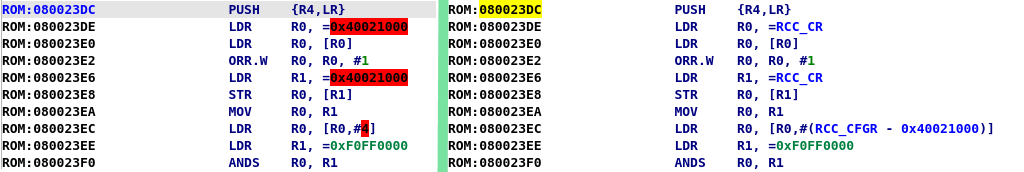
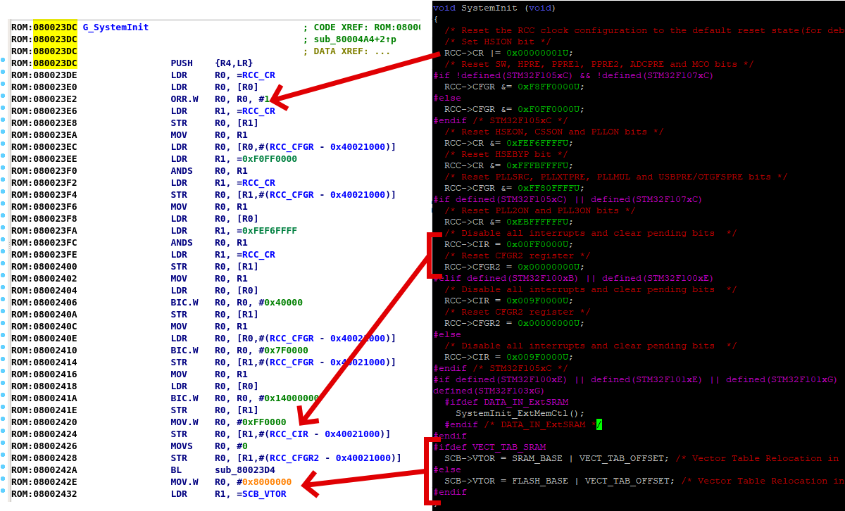
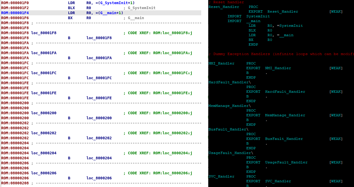
After some digging around, most of the code I locate in the first function at the reset vector looked like general setup code, this was probably generated from some boilerplate code or an IDE. The code is easily identified as such by the heavy use of the RCC (Reset and Clock Control) register, Flash registers and internal peripherals that are not supposed to be exposed to the user. To test my theory, I downloaded stm32cubemx and generated boilerplate code for the same micro-controller. As can be seen in the images below, the code that was generated is almost identical to the code at the in the first function of reset handler this proves this code is just general startup code and can be discased and not analysed. Another interesting part of the generated code was the located in startup_stm32f105xc.s where, on line 154 is the actual exported Reset_Handler symbol. Looking at the code at this location, The SystemInit address is loaded into R0 and the branched to. After the SystemInit, the main function address (__main symbol) containing the user code is loaded into R0 and branched to, this is exactly what can be seen at the reset vector in IDA. Another thing that can be seen is the bunch of dummy exception handlers after the reset vector, just like in the assembly file.
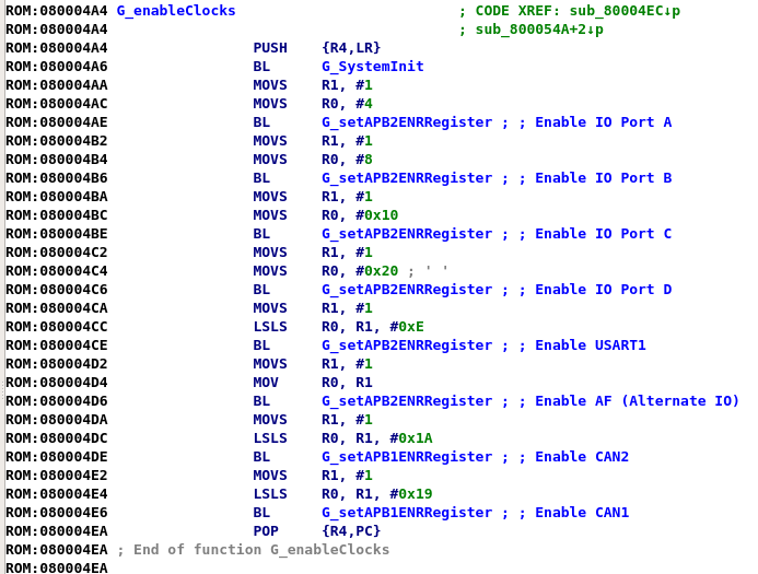
Looking into the user code at the reset vector, there is not much there either. The user code does some maintenance work such as setting up memory and initial values, after that, it enables the different peripheral clocks of the system, the first few clocks enabled are standard GPIO bus clocks, the next 2 clocks that are enabled are the CAN1 and CAN2 clocks. After the clocks are set up, the GPIO ports are setup, followed by inilization of the CAN1 interface and then the inilization of the CAN2 interface. The last thing that is set up is the USART1 port, and then the code jumps into an infinite loop that just keeps enabling interrupts on CAN1 and CAN2. The code is very lengthy, so I apologize for the lack of images.
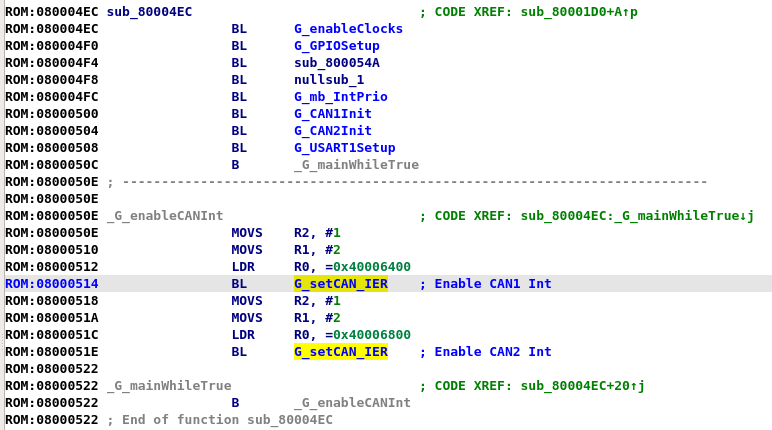
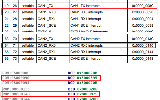
Thats all? where is the code for processing the CAN messages? The answer is in the infinite loop. Just like with any other type of communication, when the data arrives, it generates an interrupt that is handled by the code pointed from the interrupt vector table, this code is also called an ISR (Interrupt Service Routine). The offset of the CAN ISRs are located in the same table that the reset vector was found in, looking throughout the table, there are multiple ISRs that belong to CAN1 and CAN2, looking at the same locations in the loaded binary reveals that only CANx_RX0 are used for each CAN interface. Jumping to the address pointed to by the vector table (not forgetting to subtract 1 for the THUMB indicator) and converting the data to code, reveals the ISRs.
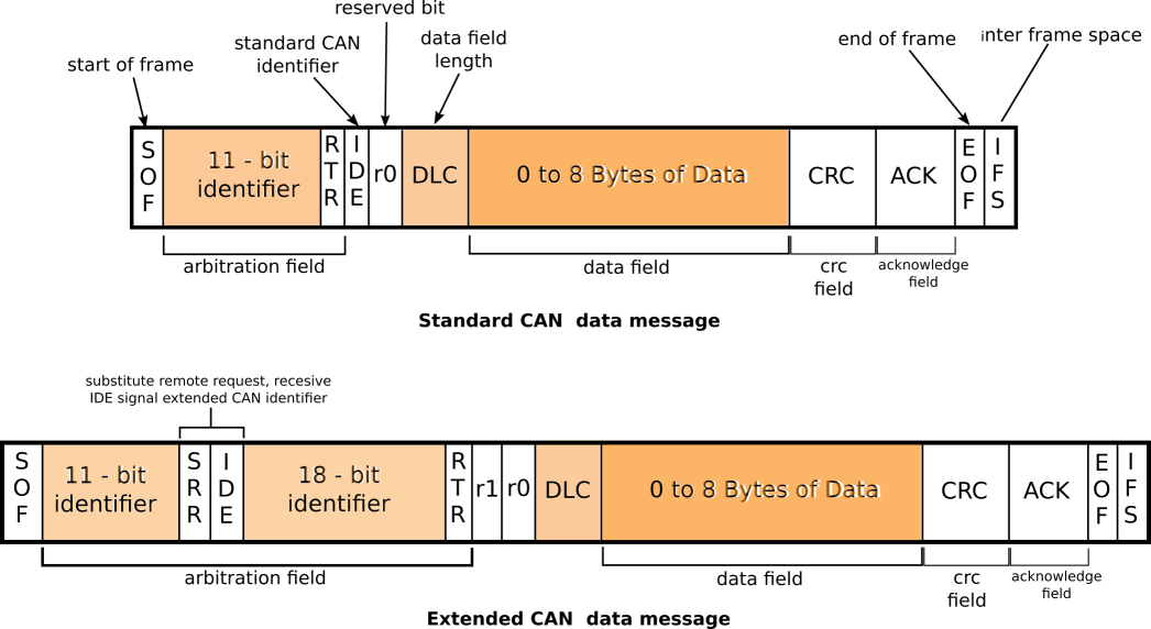
Before I continue and write about the code in the ISR, it’s probably a good idea to first understand the CAN protocol. There is no reason to repeat all the details of CAN, as it can be found and read on the Wikipedia CAN bus page. The main things to keep in mind while looking at the ISR are as follows:
- There are 2 CAN frame formats, standard and extended
- The main difference between the two is only the size of the ID (11 bits vs 29 bits)
- A frame contains the data length (DLC field) and up to 8 data bytes of payload.
- A frame can be of type “remote” only requesting data (not containing data)
The first function called from the ISR is responsible for receiving the CAN data. The function is passed 3 parameters, the first is the address of the can interfaces MCR (master control register), since the function is called from CAN2 ISR asw well, the MCP address is used as a base address for all CAN register accesses. The second argument, which is hardcoded to 0 is used as an additional offset to the CAN MCR address, the argument is used with a hard coded shift-left (basically, multiplying the value by 16). Just as the MCR is used to calculate the offset to the requested CAN registers on a specific interface, the additional offset is used to access different mailboxes on the same can interface. Looking at the datasheet for the MCU, each CAN interface has two receive slots, each slot has it’s own CAN ID and DATA registers. When the mailbox parameter is set to 1 it will access the registers for that specific mailbox on the CAN interface pointed to by the base MCR address. The third parameter that is passed to the function is a buffer in which the function copies the received data to. The receive function is pretty straight forward, it starts by checking if the Identifier extension bit (IDE) is set, then copies either 11 or 29 bits of ID data. After that, it copies in the Data length code (DLC), Remote transmission request (RTR) and the data itself (8 bytes). After the data has been copied to the buffer, it sets the RFOMx bit in the CAN_RFxR register to release the mailbox and let the hardware clear it.
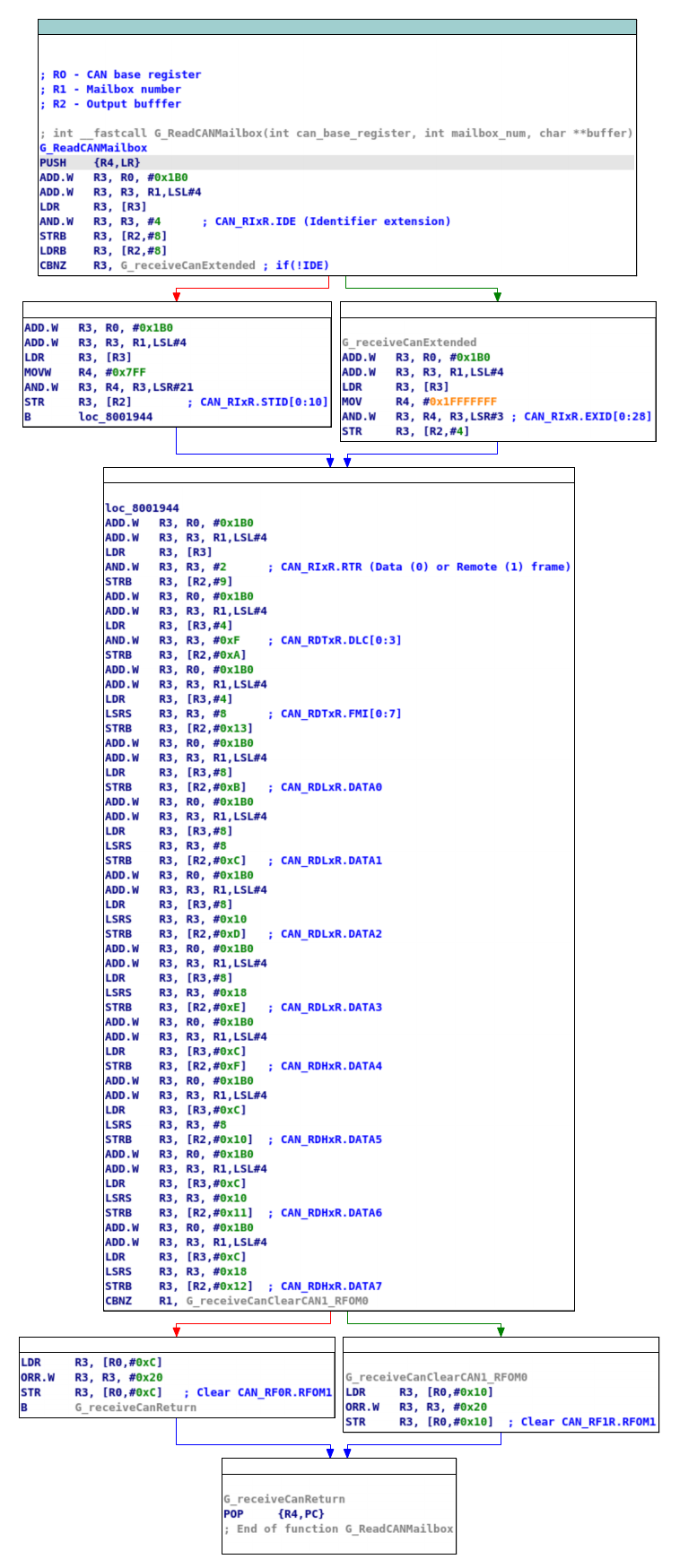
After the data has been copied, the ISR calls a second function which only disables the interrupt of the can interface that fired. The disable function also accepts the CAN MCR register as a base register and accepts a bitmask and a flag, the flag telling the function if to set or unset the bitmask in the register. The CAN interrupt is not enabled again until the ISR completes and control returns to the main user code, which is just the infinite loop that was seen before, enabling interrupts on CAN1 and CAN2 interface.
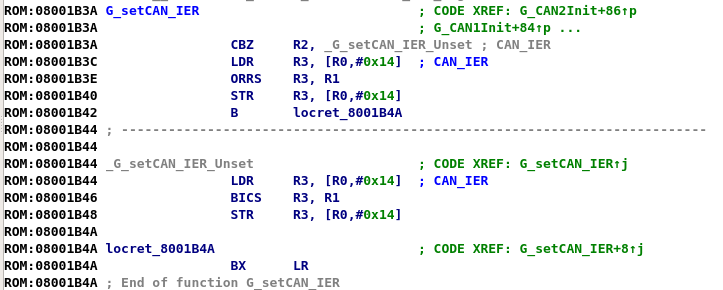
The next step of the ISR is to handle and manipulate the frame that came in. After a brief loop initializing the output buffer, the ISR starts to check the data received. A series of checks that are done by first checking the CAN ID field, if an ID field matches san ID filed that needs to be “fixed” it then checks the GPIO configuration (the hardware solder bridge pads) and tests to if the car model matches. If the car model matches, it goes on to construct the fake buffer to be retransmitted. Reconstructing this logic yields a table that reveals for each car model, what CAN ID messages it is looking for. For one car model, it seems that the ISR does some extra check on the data. If one of the configurations and CAN IDs correspond to something that needs to be handled, the ISR simply copies any unrelated data back to the fake buffer, and zeros out any other fields (that are the fields that probably contain the milage). If the data does not fit any of the criteria, it is simply sent on without any manipulation. In the table below is the summary for the frames that are caught and manipulated. The image below shows the logic code for the ISR (PURPLE- Call to receive and interrupt disable functions, YELLOW- GPIO configuration checks, BLUE- Additional DATA checks, RED-Manipulated buffer construction & call to send it).
| Car Model | GPIO Pad | CAN ID | Other Condition |
|---|---|---|---|
| Mercedes W166 | PC10 | 0x37a | N/A |
| Mercedes W222 | PC11 | 0x367 | N/A |
| Mercedes W222 | PC11 | 0x40f | N/A |
| BMW | PA15 | 0x5c0 | DATA[0] == ‘H’ |
| BMW | PA15 | 0x394 | DATA[0,1] == ‘H\0’ |
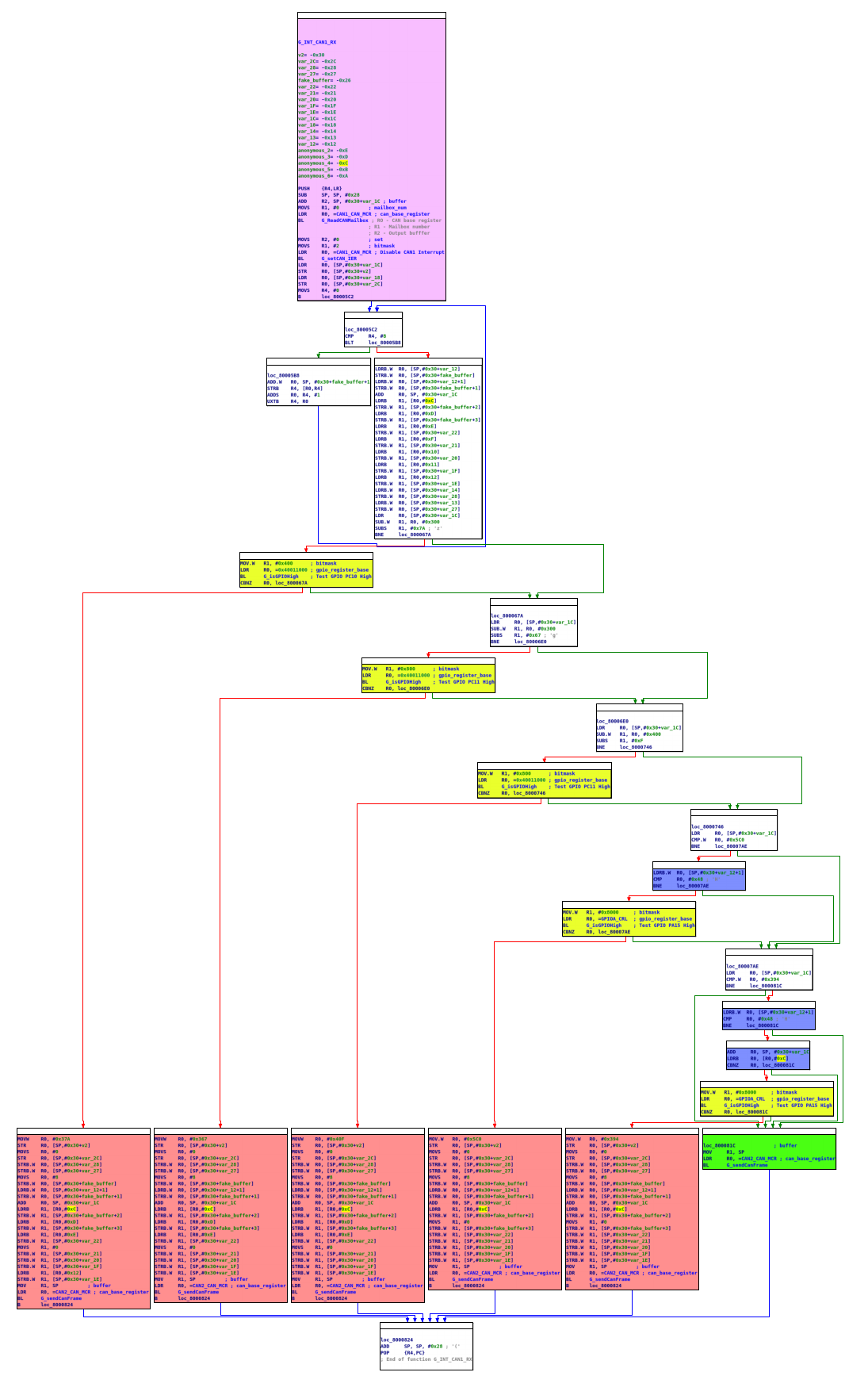
After the fake buffer is constructed, a transmit function is called that sends the fake buffer on to the other side of the CANbus. The transmit function, just like the receive function is simple, Just like the receive function, the CAN hardware has mailboxes, in the case of the transmit, there are 3 mailboxes and an empty one needs to be selected to transmit. The first thing the funrion does is to find that empty mailbox, it goes over each of the mailboxes and tests the CAN_TSR.TMEx (x=0..3), if the mailbox is ready to receive a buffer for sending, the hardware sets this bit. Just like in the receive function the code shifts the mailbox address by 4 to create an “extra offset” to the selected mailbox registers. Next the function clears CAN_TIxR.TXRQ (Transmit Request) and starts preparing the transmit registers. It loads the ID or extended ID (depending on the original frame), clears the data length register (DLC), sets up thr data itself and lastly, and sets CAN_TIxR.TXRQ to 1 requesting the hardware to send the frame. And that is basically all, once the transmit function retuns to the ISR the ISR has done it’s job.
Looking at the ISR for the second second CAN interface, it’s overall the same, only the logic for selecting the frames is different, the second ISR logic table is as follows:
| Car Model | GPIO Pad | CAN ID | Other Condition |
|---|---|---|---|
| Mercedes W166 | PC10 | 0x3d9 | N/A |
| Mercedes W166 | PC10 | 0x19f | N/A |
| Mercedes W222 | PC11 | 0x367 | N/A |
| Mercedes W222 | PC11 | 0x40f | N/A |
| BMW | PA15 | 0x330 | N/A |
| BMW | PA15 | 0x5c0 | DATA[0] == ‘H’ |
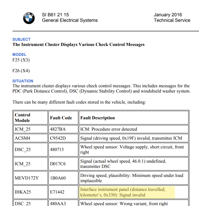
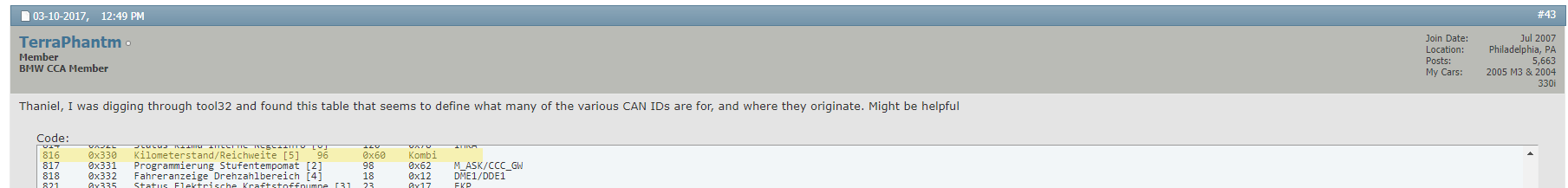
It is interesting to note that for the fourth configuration jumper (PC12) I could not find any code, so I don’t think the board actually supports it. As I don’t own any of the cars that are supported by the board, I could not sniff the CANbus and see an actual frame on the bus, I did try to Google some of the CAN IDs, but did not find any good information about them, only some limited information about the BMW codes (see images below), but I guess they are the important messages when it comes to reporting to the instrument cluster. Since the device only sits between the instrument custer and the ECU, I don’t think it has the ability to persistently fake the mileage on the car (as Big Clive stated that after the device was removed, an additional 40k appeared on the odometer).
Conclusion and notes
Legality aside, it’s a dangerous game to connect these type of devices to critical systems (such as a car). The devices are cheap and I’m guessing do not conform to any vehicle safety standard for electronics. Looking into this device gave me the option to explore the CAN interface on the STM32F more deeply, and to be honest, I think with some code modifications this device can make an excellent platform for toying with CANbus, after all it has all the hardware needed and even provides 2 interfaces. Maybe I’ll write some code in the future to interact with it over serial.
I was also very pleased to find the the Nucleo board I ordered (with the ST-Link capable daughter-board) was compatible and I did manage to read, write and even run a DGB session interacting with the device. I would liked to also be able to test my theory and send the device some can messages, to see if it responds as I think it should, but as I mentioned before I do not have the hardware (yet). I would also like to remind anyone reading that the video that Big Clive made was the inspiration for this reversing project, and encourage you to checkout the video.
Until the next time…