Inside a Switcher V2 - Part 2, Mapping and Extracting
After going over the Switcher’s overview and internal components in part 1 it was time to take a closer look at the specifics of each component. The first thing on the list was to map out the main functions of the I/O pins on each of the chips (the Espressif ESP8266 and the Nuvoton N76E003). As I determined in the previous post, the N76E003 is used as a controller some of the components such as the power monitoring chip and relay. I took some images of the boards, and with the help of the images and a multimeter and logic analyzer I mapped out the function of each I/O pin on the microcontrollers. In order to understand the type of I/O used, I referenced the Nuvoton N76E003 data-sheet (page 10, figure 4-1), and the Espressif ESP8266 data-sheet (page 4, figure 2-1). I created the following table, describing the major I/O lines on the logic board:
| MC Type | Pin# | Name | Function |
|---|---|---|---|
| ESP8266 | 24 | GPIO5 | Wifi/Rest Button |
| ESP8266 | 16 | GPIO4 | Manual On/Off Button |
| ESP8266 | 15 | GPIO0 | Header marked “DWN” |
| N76E003 | 02 | TXD | Serial Tx |
| N76E003 | 03 | RXD | Serial Rx |
| N76E003 | 10 | P1.5 | Wifi Status LED |
| N76E003 | 01 | P0.5 | On/Off Status LED |
| N76E003 | 16 | P0.0 | 30-45min status LED |
| N76E003 | 17 | P0.1 | 45-60min status LED |
| N76E003 | 13 | P1.2 | 15-30min status LED |
| N76E003 | 12 | P1.3 | 0-15min status LED |
| N76E003 | 15 | P1.0 | HLW8012 Energy monitor “CF” line |
| N76E003 | 14 | P1.1 | Mains power sense? (not sure) |
| N76E003 | 19 | P0.3 | Relay enable line |
| N76E003 | 20 | P0.4 | connected to ESP8266 CHIP_EN pin |
| N76E003 | 06 | P1.4 | connected to ESP8266 EXT_RSTB pin |
A small note about the mapping I created, I am not to sure what the function of P1.1 (14) on the N76E003 is, it’s connected via an optocoupler to the mains board, and seems to be wired between the input LINE (250vac in) and the output NEUTRAL (boiler side). It may be some kind of mains power sensing. The other odd thing I noticed was that the serial lines (Rx/Tx) were connected to both microprocessors. My guess is that this serial line is used for communication between the ESP8266 and the N76E003, knowing this, it explains the garbage data I saw when connecting to the serial header, it must be a binary protocol, and maybe also at a different baud rate.
My next step was to extract the firmware from the two microcontrollers on the board, the first I extracted was the ESP8266, I had 2 options, either dump the flash via the bootloader with esptool or connect directly to the external SPI flash chip. I decided to start with the former, by connecting to the Rx,Tx and DWN pins (DWN allows to set ESP8266 GPIO05 low, enabling flash mode), I then proceeded to use esptool to connect to the chip, and dump the flash data with the read_flash command: python ~/tools/esptool/esptool.py --port /dev/ttyUSB0 --baud 921600 read_flash 0x00000 0x100000 switcher_esp_fw.bin. You might notice that I used a ludicrous baud rate of 921600, that is due to the N76E003 sending periodic messages on the serial lines, which were messing up esptool and causing it to either get stuck or abort. Later on, I found a way to shut down the N76E003 chip, and to dump the flash at a lower, safer baud rate.
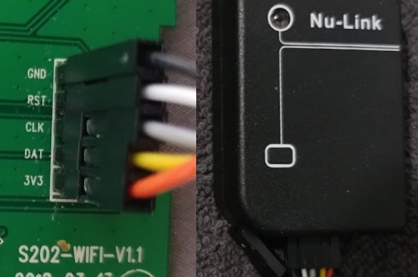
The next firmware I need to dump is the N76E003s. Unlike the ESP8266, the N76E003s ROM is internal, so I don’t have the option of piggybacking on to the SPI bus of the chip. Another snag is that I could not figure out if the serial interface will allow reading the ROM. Reading through the datasheet, I found that there is some serial programming support, but could not figure out the exact way or scenario it can be used in, On page 246 of the datasheet, I came across ICP (In Circuit Programming) as the datasheet claimed ICP method makes it easy and possible without removing the microcontroller from the system, so I opted to try it. I decided to buy a cheap (knockoff?) Nuvoton ICP programmer called Nu-Link and use it with the Nuvotons software. Looking at the ICPs pinout, I saw that some of the header names are familiar, the CLK,DAT,RST lines all had header connections on the board, it seems to be that each row of headers on the logic board correspond to each chip.
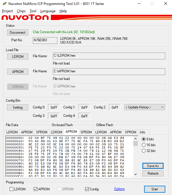
After I downloaded and installed the software on my computer (can be found here) I connected the device to the computer and started the program. The first this was to select the target chip type, which I got from the datasheet as a “T1-8051” and the software language. After that, clicking on the “connect” button and some annoyance about the chips firmware (I guess the bootloader) was not up to date, I got a promising Chip connected with Nu-Link (ID:181002ed) message. Down at the bottom of window, there was a few tabs, grouped into File Data, On-board Flash and Offline Flash. Under the On-board Flash section, I selected the APROM (Application ROM) tab and clicked on refresh. It took a second or two, but on the screen a beautiful hexdump of the chips firmware appeared. I saved the firmware with the Save As button and went to celebrate.
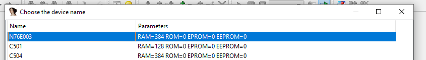
After getting the firmwares successfully, it’s time to see what is inside them. I decided to start off with the N76E003 firmware, as it intrigues me to what it’s function. From the datasheet, I know it’s an Intel 8051 based processor, so naturally I selected this processor in IDA. After proceeding and creating the ROM sections, I was prompted to choose a device type, this was a problem. The device types are ties to individual implementations of the 8051 architecture. I tried to use some common/default devices types, all parsed the opcodes correctly, but the SFR (Special Function Register) names were either wrong or missing. It seems I will need to create my own device definitions specifically for the nN76E003 8051 architecture.
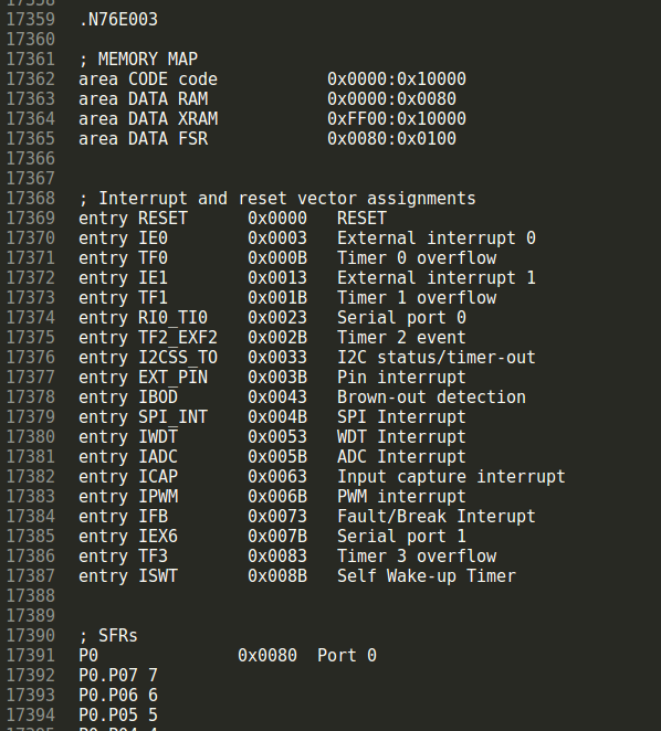
I started to look into IDA configurations and plugins, in the IDA SDK I found the code responsible for the 8051 disassembling under <idasdk-path>/module/i51. The file i51.cfg can also be found in the cfg directory which is under the IDA install directory. Looking at this file and the documentation, I added my own device type to the 8051 module. I started by defining the device name .N76E003, and using the N76E003 datasheet, I followed with area definitions for the memory map (pages 15-17 of the datasheet), continued with entry definitions for interrupts/reset vectors (page 199, Table 20-1) and finished with a really long list of I/O and SFR definitions (page 20, Table 6-1). I also used table Table 6-2 from pages 21-24 to descriptions and bit addressable entries to the configuration. At the end of all this, I had a 8051 device definition that suites the N76E003. The full configuration I write can be found here. I reloaded the firmware into IDA, and this time selected the device I added.
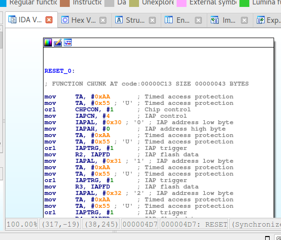
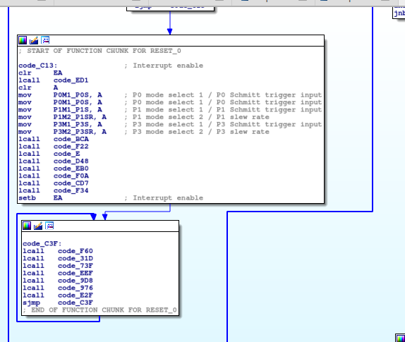
No that I have all the correct SFR names, It was time to start reversing the firmware. I followed a jump from the reset vector and started looking for interesting paths. The first few code blocks are all to do with setting up the chip, I skipped these for now, as I don’t really care (yet) what clock diviser is selected for the system clock. Browsing down a bit, I saw a few references to P0M0 and P1M0 and more, from reading the datasheet I knew these were the I/O port mode selection, and from the pinout of the device, I know that the I/O ports are used extensively. Following the code down, There is an infinite loop with a bunch of function calls in them, this is typical of microcontrollers, and this is where the core of the logic it. I decided to name the one-off function calls as setup and the main loop as loop and started to disassemble the function.
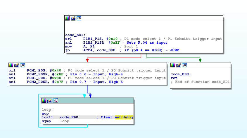
Earlier on, I wrote that I found a better way to dump the ESP8266 firmware without the N76E003 interfering. In the setup area, the function located at 0x0ed1 checks the state of P0.4 (Port 0, Bit 4) and if it sees that the port is logic LOW it sets P0.6 and P0.7 to be inputs with high-impedance and then falls into an infinite loop (clearing a watchdog timer). This is great news! as P0.6 and P0.7 are the Rx/Tx lines of serial0. Again, I used a multimeter and found that P0.4 is connected to the testpads named TEST on the board. Now, every time I want to only access the ESP8266, I can keep the testpad TEST low and stop the N76E003 from interrupting. I checked this out, and sure enough it works, I can communicate with the ESP8266, and none of the LEDS light up, meaning the N76E003 is inactive.
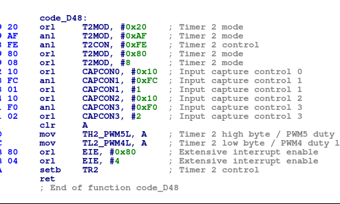
Continuing down the code, there are multiple functions to set GPIO default states and directions, and then come some more interesting functions. from function 0x00E (which sets up timer 0) things get even more interesting. Function 0x0d48 start setting up timer-2 and a capture channel with interrupts, after setting up the timer and capture parameters, it specifies via CAPCON3[0:3] that the capture channel on P1.0, this is the pin that is connected to HLW8012 energy monitor chip, specifically the CF pin on that chip.
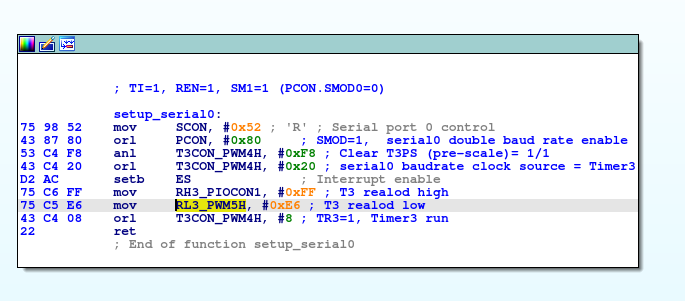
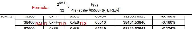
Another interesting function to look at is located at 0x0f0a. This function sets up serial port 0. It uses SCON and PCON to setup the serial0 and using T3CON,TH3 and TL3 to setup Timer3 as a baud-rate clock source. On page 129 of the datasheet, there is a handy formula and table to determine the baud-rate from the values used in the code (Formula no. 4, Table 13-3). By plugging in our values, or looking them up on the second table, the baud rate of the device turns out to be 38400 (actually, 38461.53846). This is good to know, as it gives us a hint to what baudrate to look for on the ESP8266, and also allows us to know what baud rate to use when trying to decode the N76E003 serial messages.
After the serial setup, there are some more functions, such as 0x0cd7 which sets up the watchdog timer that resets the chip if it gets stuck or in an unknown state (this watchdog needs to be cleared if entering an infinite loop, as seen before in 0x0ed1) next the device sets up interrupt priorities (function 0x0f34) and enters the main control loop (at 0x0c3f).
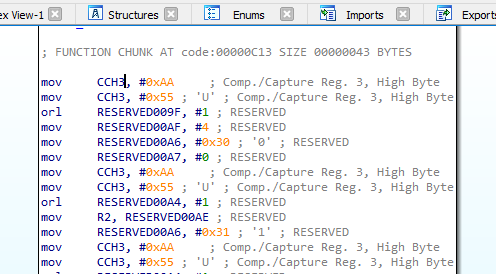
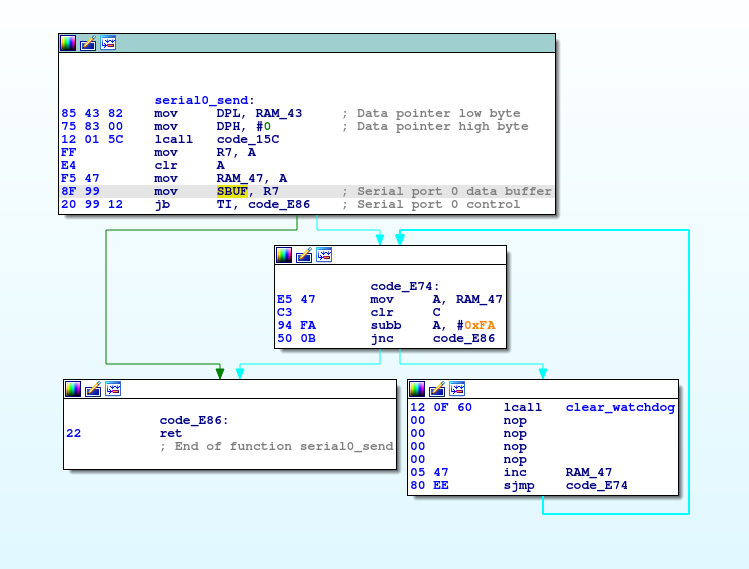
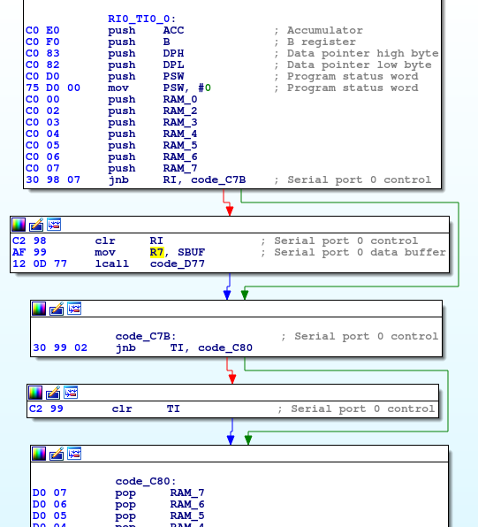
I have not yet studied the control loop, but the first function that is called is to clear the watchdog timer and after that it seems there is some logic running, manipulating the different I/O ports of the device. Once I look further into the control loop, I’ll write a new post about it. Since I looked at the vector and interrupt addresses in order to create the device configuration for IDA, I did have a chance to peek at the different interrupts and found the serial transmit and receive handlers. As seen in the images below, the serial send function is located at 0x0e62 and the serial receive handler is at 0x0c56, it is clearly visible the difference between the send and receive function, the send function looks like any other function, but the receive function is an interrupt handler so it pushes all the registers (including the PSW (Program Status Word)) onto the stack and pops them all back off at the end. Another small difference is the use of the reti instruction (return interrupt) instead of the standard ret (return) instruction. These differences can also be spotted in the capture interrupt (at 0x05db) and more.
I think this post needs to come to an end, in this post, I started with mapping out the different I/Os, extracting firmware from the two microcontrollers on the board, creating a custom IDA device configuration to load the firmware of the N76E003, and then starting to disassemble it. It’s only the beginning of the process to understand the function of the N76E003 chip, but I will carry on as time goes by. I will also eventually load the ESP8266 firmware and take a look at that too. Looking forward to writing more in my next post.