Inside a Switcher V2 - Part 1, Overview
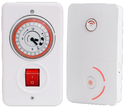
On advice from a friend, I ended up buying a Swticher V2 to connect to an immersion heater and replace the analog timer with a more modern digital one, which contains features such as timer mode, scheduler and power consumption calculator. The device itself uses WiFi to connect to the home network and has a complementary phone app o control it. The device costs approximately 70 US$ and to my opinion is no more than a glorified Sonoff with a few extra LEDs. In this post, I’ll take apart he device and have a peek inside it. Before I dive any deeper I would like to make two things clear:
- I am no electrical engineer, it’s just a small hobby.
- Even though the device does it’s job, it’s price compared to a 15 US$ Sonoff is a ripoff. Especially given the pain in the ass phone app.
Before taking the device apart, and potentially destroying it, I setup the device on my local network and tested it’s functionality. After much effort, blood, sweat and tears it finally connected to my network and I got the device working. I tested all functionality such as the auto-shutoff, scheduled start/stop, timer and on/off and made sure the device was working as expected. After that, it was time to have a closer look under the hood.
The device is made out of cheap ABS(?) plastic and is held closed by a four self-tapping screws on the back. Once the screws are out, the clam shell can be removed to expose the boards. Once opened, I found two PCBs inside. It seems that the device has a high-voltage switching side and a low-voltage logic side. I’m to exactly sure if it’s the reason for 2 PCBs, since the track spacing between the mains leads and the leads feeding the logic board is quite narrow and with no isolation cuts. Then again, I’m no electrical engineer.
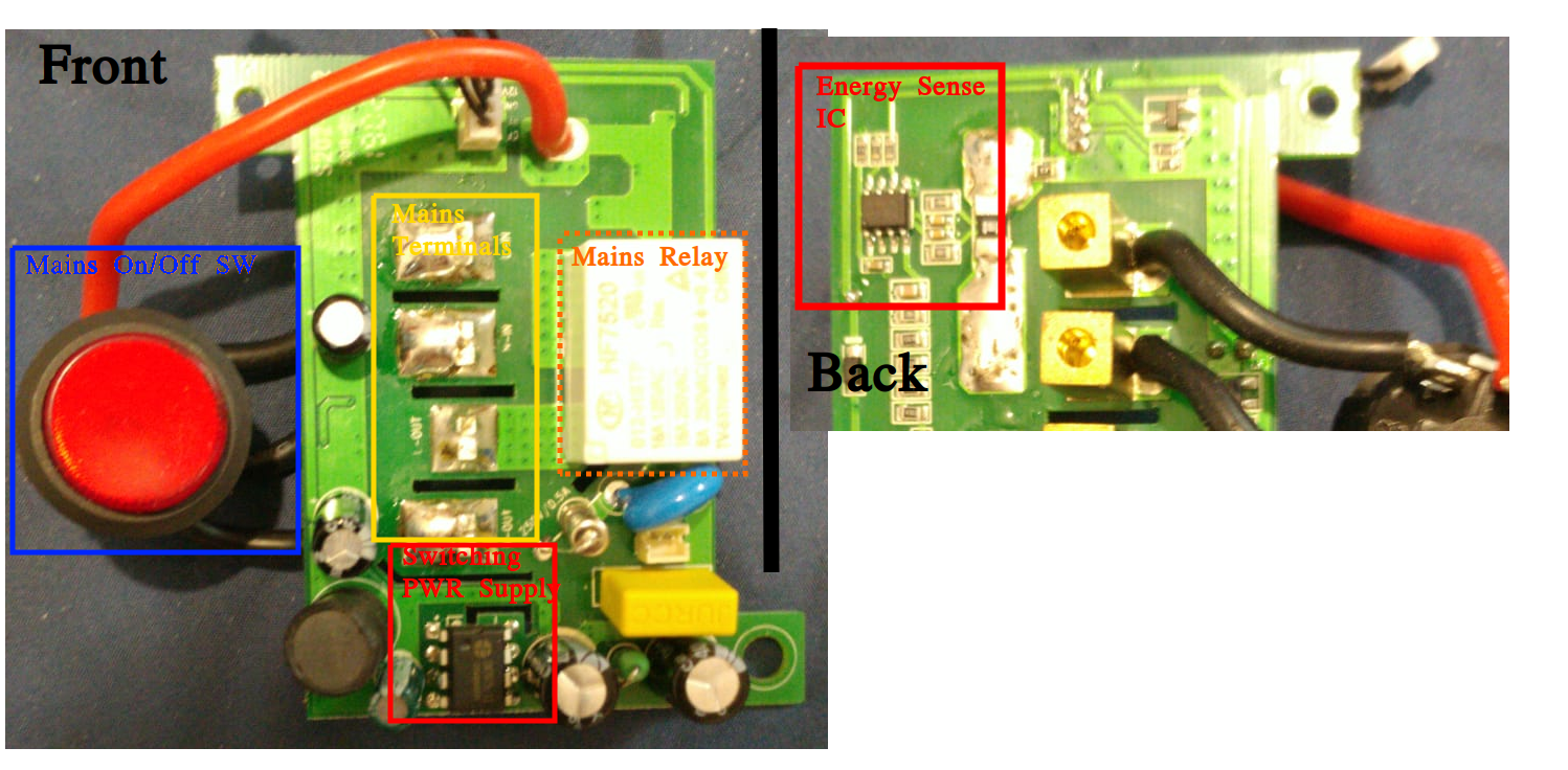
So what exactly makes a Switcher tick? The mains board consists of the mains input posts, a big (cheap) illuminated button, 16A/250V relay, a SW7075-12 12v switching power supply, and one HLW8012 single phase energy monitor IC. On the logic board, there are 6 LEDS, 2 tactile buttons, an ESP8266 as the brains, an N76E003, and one itty bitty 1MB 25d80 flash chip. One more welcomed feature on the logic board is a 10 pin header, probably for debug or flashing. You also might have noticed, these are components you will find in a Sonoff and other cheap (less than 70 US$) IoT devices.
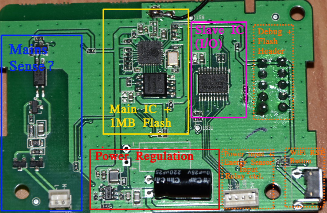
The first thought that went through my head was “Can I connect to the serial port?” and the second thought was “Why does it have two ICs?”. After some messing around and tracing some of the races on the board, I have noticed that all the LEDs on the board are connected to the IO pins of the N76E006. My current assumption is that the N76E003 is used as some sort of IO expander, though I can figure out why not use a PCF8574 or somting of the sort. Edit: I hav also noticed that the relay and current mesurment IC are connected to the N76E003
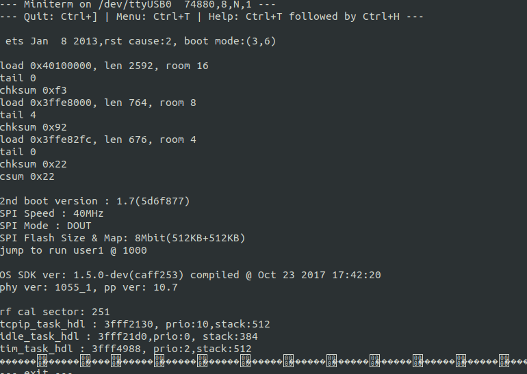
As to my second thought of connecting to the the serial port of the device, from the markings on the header pads it seems it may be a possibility, so I soldered on some header pins and connected the device to a cheap serial to USB adapter. I decided to open the serial port with a 115200 baudrate, as this is a common speed. The first thing I noticed was that I was getting a bunch of garbage, there was no sense in the serial information. I played around with the baudrates but no luck, it all still seemed like junk. I then noticed a familiar pattern, each time the the WiFi LED blinked a small packet of data was sent on the serial port. This may be the ESP8266 sending the N76E003 a signal to turn on the LEDs, if the ESP8266 reset pin was held low, everything froze in place, and the LEDs stopped the blinking. After some fiddling about and trying different baudrates I did get a readable response from the ESP using a baudrate of 74880. This baurate stems from a miscalculation in the ESPs bootloader (as far as I know). But after all that, there are still some packets that I cannot understand, it seems to be a binary protocol. But thats a problem for later.
Once I saw their was no meaningful way of communicating with the device over the serial port, I decided to map out the board more extensively. I traced most of the connections on the board and documented them them to benefit further research. Posted below is an image of the logic board split into logical blocks. The only part of the board that i’m not sure about is the isolated area labeled mains sense? in the image. It seems that the mains (line and neutral) come in to operate a optocoupler that is fed back to the N75E003. I guess I’ll find what it’s about later.
In the next part, I’ll talk about the general layout of the board, attempting to read the flash from the device and hopefully even start to reverse engineer he firmware.